Huawei’s ‘Tau Law’ Gambit: Building Technological Self-Reliance on the Foundation of Scale

Authored On
Modified
Huawei declares its goal of achieving 1.4-nanometer-class chips by 2031
China seeks to bypass EUV constraints through Logic Folding design architecture
Aims to narrow the technology gap through accumulated manufacturing experience
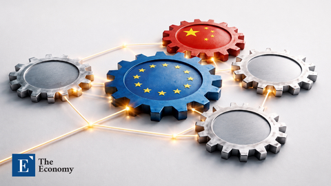
Huawei, the driving force behind China’s indigenous semiconductor industry, has proposed a new semiconductor development theory, and a world-renowned scholar has formally endorsed its theoretical feasibility. While the United States has sought to restrict China’s access to leading-edge process technologies by blocking exports of advanced semiconductors and manufacturing equipment, China has accelerated efforts to establish a self-sufficient ecosystem spanning chip design, manufacturing, equipment, and materials. The theory unveiled by Huawei is likewise viewed as a new semiconductor development pathway emerging from this broader self-reliance strategy. Industry observers largely agree that it remains premature to discuss technological achievements capable of replacing existing market standards, yet there is little disagreement that China is mobilizing national resources to build an entirely new technological framework.
EDA Authority “Tau Law Roadmap Is Realistic”
EDA Authority “Tau Law Roadmap Is Realistic”According to Chinese IT media outlet MyDrivers on June 8, Andrew B. Kahng, Distinguished Chair Professor at the University of California, San Diego and one of the world’s foremost authorities in electronic design automation (EDA), recently stated that “Huawei’s independent path is entirely achievable.” After analyzing Huawei’s newly established scaling roadmap, Kahng explained that the company has already secured a verifiable pathway capable of delivering a 1.4-nanometer-class technological leap within five years. The assessment marks a rare public acknowledgment that China has reached a far more advanced stage of design autonomy than many Western academic forecasts had anticipated.
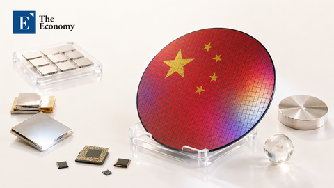
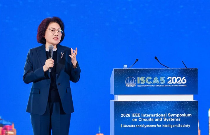
Last month, Huawei presented its new semiconductor development theory at the 2026 International Symposium on Circuits and Systems (ISCAS), hosted by the Institute of Electrical and Electronics Engineers (IEEE) in Shanghai. What captured industry attention was Huawei’s proposal of the “Tau Scaling Law” as an alternative to the semiconductor industry’s longstanding benchmark, Moore’s Law. Whereas Moore’s Law posits that integrated circuit density doubles roughly every 18 to 24 months, delivering higher performance at lower cost through relentless miniaturization, the Tau Law seeks to transform performance gains into reductions in signal transmission time through technologies such as Logic Folding. Rather than relying exclusively on geometric scaling, the theory aims to enhance performance by compressing the effective tau constant across every layer of the stack, including devices, circuits, chips, and systems.
Previously, He Tingbo highlighted the limitations of Moore’s Law in a paper titled “Time Scaling Theory for Multilayer Electronic Systems,” arguing that “the economic returns of pure geometric scaling have steadily diminished beyond the 7-nanometer node.” Analyses indicate that depreciation costs for extreme ultraviolet (EUV) lithography equipment and growing design-rule complexity have already pushed the development budgets of leading-edge 2-nanometer chips beyond $1 billion. At the core of the Tau Law is Logic Folding. The approach stacks digital circuits, analog circuits, and memory circuits across multiple layers and connects them through ultra-fine hybrid bonding. According to Huawei, this architecture reduces signal travel distance, minimizes power losses and interference during transmission, and ultimately shortens signal propagation time itself.
China Expands Semiconductor Manufacturing Base Amid Equipment Restrictions
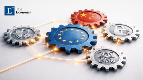
The proposal has attracted particular attention because it represents an attempt to overcome China’s most significant bottleneck—the inability to import ASML’s EUV lithography systems, which remain indispensable for conventional integrated circuit miniaturization—through system-level optimization technologies. Industry analysts interpret Huawei’s announcement as a declaration that China intends to reduce its semiconductor technology gap with the West from roughly five years to approximately three. While the United States and its allies continue restricting access to advanced equipment, China is simultaneously pursuing alternative design methodologies, legacy-generation DUV multipatterning, advanced packaging, domestic equipment development, and next-generation light-source research. The broader objective is to address technology bottlenecks created by U.S. export controls through multiple state-backed channels.
China’s semiconductor self-sufficiency strategy combines technological workarounds with an extensive industrial subsidy framework. According to Reuters, China established the third phase of its National Integrated Circuit Industry Investment Fund in 2024 with capital totaling approximately $48 billion. With contributions from the Ministry of Finance, local governments, state-owned enterprises, and state-owned banks, semiconductor support has evolved into a national initiative integrating central government resources and policy finance. The latest fund is directed primarily toward manufacturing capacity expansion and equipment localization. While the first and second phases focused on expanding foundry and memory manufacturing capabilities, the third phase concentrates on strengthening lithography, etching, deposition, inspection equipment, and the broader ecosystem of materials and components.
The support structure extends well beyond direct subsidies. Chinese authorities have long provided semiconductor equipment companies with tax incentives, free or discounted land, government grants, and equity investments. This framework reduces the burden of short-term losses and creates financial buffers that allow companies to pursue long-term yield improvements and equipment development. Capital expenditure trends reinforce this strategy. According to the Center for Strategic and International Studies (CSIS), China’s semiconductor equipment spending reached $49.3 billion last year, declining only 0.5% year over year while remaining near historic highs. Chinese companies continued investing heavily in both mature-node production and selected advanced manufacturing capabilities.
State-Backed Scale Intensifies Pressure on the Technology Gap
These investment flows are increasingly reshaping pricing dynamics across lower-cost market segments. Mature-node semiconductors serve a broad range of applications, including automobiles, home appliances, industrial electronics, and power management chips. While technological barriers remain lower than those of advanced nodes, the impact of oversupply can be substantial. Chinese firms are already expanding faster than many industry forecasts anticipated. According to Counterpoint Research, China’s leading DRAM manufacturer, ChangXin Memory Technologies (CXMT), increased first-quarter revenue by more than 700% year over year, lifting its market share to 8%. The gains were driven by rising domestic demand for smartphones and servers, alongside higher memory prices.
In the NAND market, Yangtze Memory Technologies (YMTC) delivered some of the strongest performance. The company’s first-quarter revenue surged 445%, raising its market share to 13%. Its share stood near 8% a year earlier, meaning it gained five percentage points within a single year. China’s rise is also becoming increasingly visible in the foundry sector. According to TrendForce, the market-share gap between Samsung Electronics (7.1%) and China’s largest foundry, Semiconductor Manufacturing International Corp. (SMIC, 5.2%), narrowed by 0.7 percentage points year over year as of the fourth quarter of last year. SMIC is currently focusing on improving yields for 7-nanometer manufacturing processes, moving beyond mature-node production toward more advanced capabilities.
The competitiveness of China’s semiconductor industry stems in large part from its state-backed industrial mobilization system. Building a single semiconductor fabrication plant requires tens of billions of dollars in investment, while yield stabilization can take years. Few countries possess the capacity to absorb prolonged losses while continuously expanding production. In China, central and local governments, together with state-owned financial institutions, collectively provide funding and absorb much of the associated burden. This structure enables companies to prioritize manufacturing capacity expansion and market-share gains over short-term profitability.
Another pillar supporting China’s semiconductor industry is its overwhelming cost competitiveness. Although advanced semiconductor production lines are highly automated, large workforces remain essential for production management, process operations, equipment maintenance, backend manufacturing, and packaging. In South Korea, the United States, Japan, and Europe, rising labor costs and investment burdens increasingly constrain capacity expansion. China operates under different conditions. The combination of central and local government support, policy financing from state-owned financial institutions, and a vast manufacturing labor pool has created a framework capable of sustaining long-term investment growth.
This environment allows Chinese companies to continue expanding production capacity without being derailed by short-term earnings fluctuations. Semiconductor manufacturing is an industry where output volume itself becomes a source of competitiveness. As production increases, process data accumulates. Accumulated data improves yields, and higher yields reduce manufacturing costs. Lower production costs, in turn, strengthen price competitiveness. Chinese semiconductor companies are constructing this virtuous cycle under the umbrella of state support.
This dynamic helps explain the aggressive expansion of Chinese firms in mature-node markets. Commodity semiconductors used in automobiles, industrial equipment, consumer appliances, and telecommunications systems are often highly sensitive to pricing. Huawei’s Tau Law emerged from this industrial foundation. China is currently pursuing design optimization, advanced packaging, equipment localization, and mature-node capacity expansion simultaneously. The manufacturing experience and financial resources generated through capacity growth have become the foundation for the development of new technologies.
Similar Post